Copyright 2019 Reflux Design
Interactive Map by Carl-Friedrich Schön
Mission of the Institute
The mission of our institute is to design advanced functional materials with superior properties, including phase change materials, solar cells and thermoelectrics. While we share this goal with many other research groups in industry and academia, our vision how to reach this goal differs.Our approach is to devise (treasure) maps, which exploit the close relation between stoichiometry, chemical bonding and the resulting material properties. In contrast to previous maps, which were based on empirical (atomic) properties and did not consider the atomic arrangement, we have developed a novel material map, which is based on quantum-chemical calculations considering the atomic positions in the solid. This map possesses remarkable predictive power and shows that many phase change materials, thermoelectrics and photovoltaic materials are located in well-defined regions of the map.
A Treasure Map for Materials
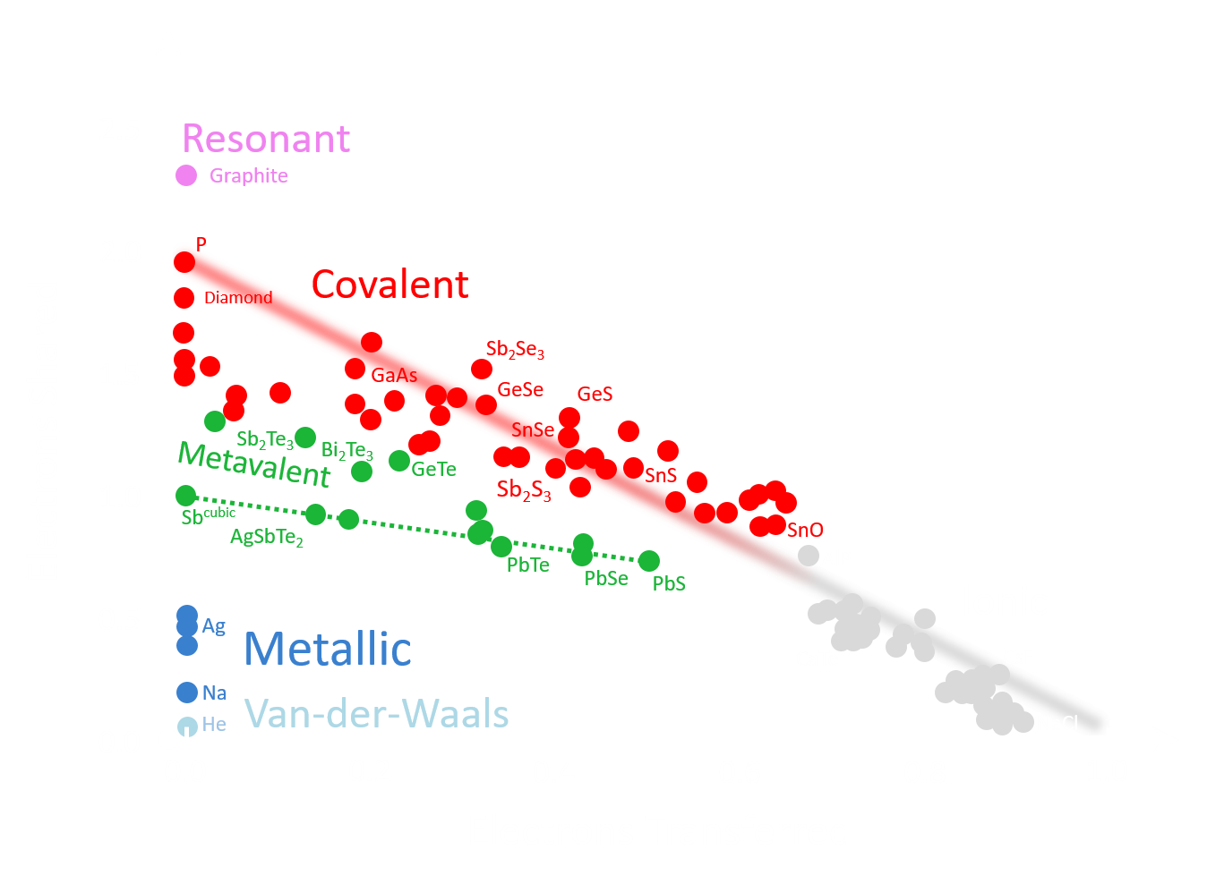
Our approach uses two coordinates, the number of electrons transferred (ET) and the number of electrons shared (ES) between adjacent atoms. These values are derived from quantum-chemical calculations. An ES value of 2 corresponds to a perfect covalent bond with one electron pair being shared between adjacent atoms, while an ET value of 1 indicates that the valence electrons are fully transferred, forming a perfect ionic bond. This map can separate clearly between classical chemical bonds, such as metallic, covalent and ionic bonds and indicates that another fundamental bonding mechanism exists in solids, which has been coined Metavalent Bonding.
Visualization is Key
An interactive version of this map has been created to reduce the entry barrier of utilizing our concepts. On startup, the 2D map representation using ES and ET is shown. The view can be rotated by holding down the right mouse button. Left clicking a data point opens a panel with additional information about the material selected. To transition between different map types: 1st generation: van Arkel / Ketelaar; 2nd generation: Philips, van Vechten, Littlewood; 3rd generation (based on ES and ET: our work) the green buttons on the left hand side can be clicked. The blue buttons at the top display various properties on the z-axis. Hovering over a button opens a tooltip with a description of its function.
What We are Good at
We are innately curious: we spend lots of time identifying exciting questions to tackle and then work very hard to reach clear-cut answers using well-designed experiments.Where Matter Matters
The preparation of samples with interesting properties is of paramount importance for our team. We either produce thin film samples with the desired stoichiometry and exciting properties by molecular beam epitaxy or sputtering or grow our own single crystals.
Looking Beyond the Bond
Our work builds on the belief that optical properties are governed by the chemical bonds between the atoms involved. Hence, we measure optical properties with high precision using FTIR spectroscopy, spectroscopic ellipsometry as well as UV / VIS spectroscopy.
Where Every Atom Counts
We need to determine the stoichiometry of our samples with great precision. Yet, beyond this, we also want to determine the atomic arrangement on the nanoscale, enabling us to detect sample inhomogeneities and nanostructures employing atom probe tomography. Needless to say that we also determine the average atomic arrangement with high precision using x-ray and electron diffraction.
From Bonds to Bands and Back
We need to determine the stoichiometry of our samples with great precision. Yet, beyond this, we also want to determine the atomic arrangement on the nanoscale, enabling us to detect sample inhomogeneities and nanostructures employing atom probe tomography. Needless to say that we also determine the average atomic arrangement with high precision using x-ray and electron diffraction.
Our Work
A few selected publications are shown below:
Atom Probe Tomography: a Local Probe for Chemical Bonds in Solids
Advanced Materials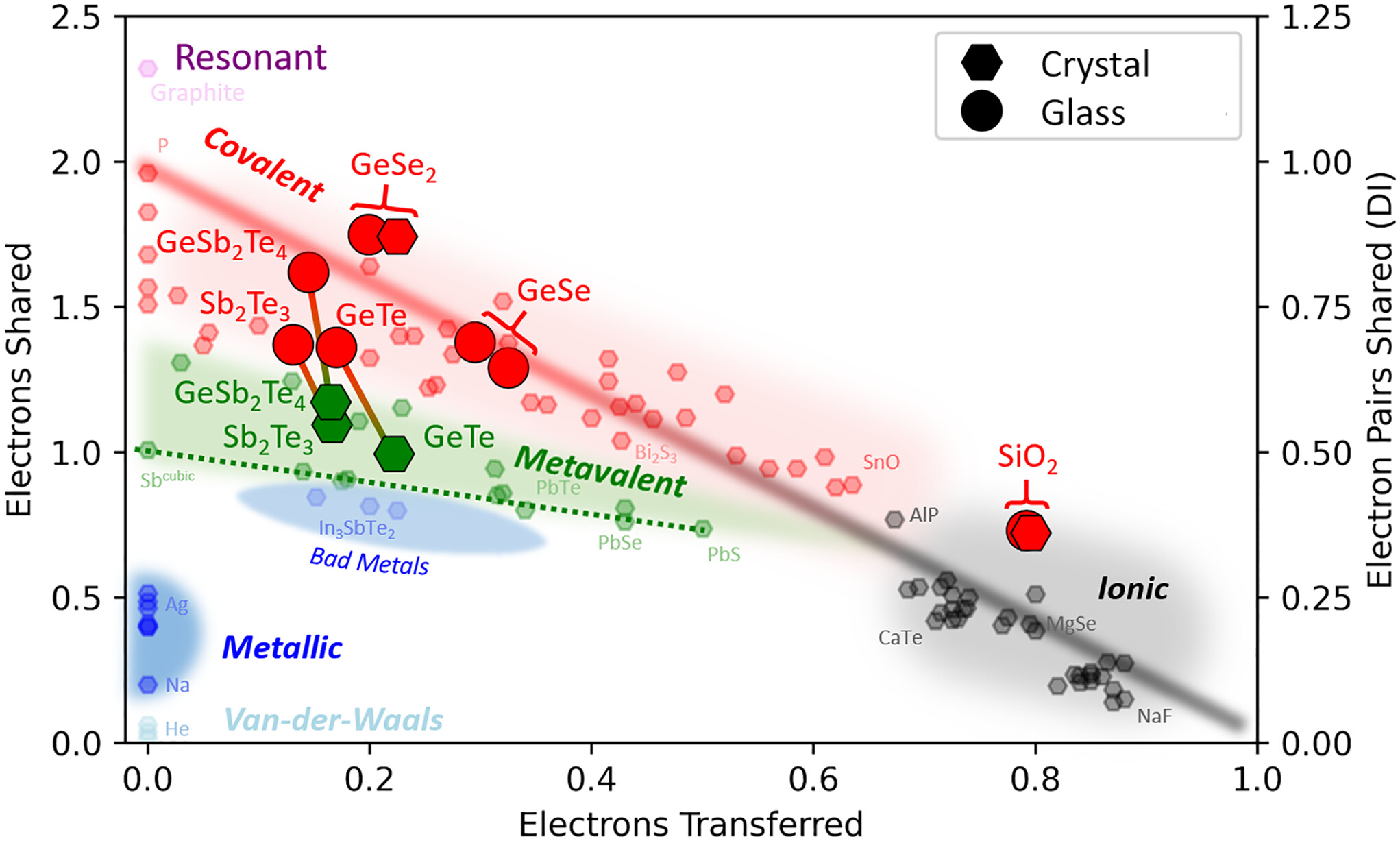
Tailoring chemical bonds to design unconventional glasses
PNAS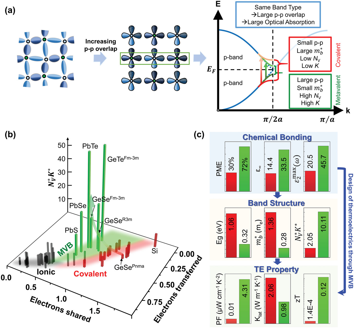
Doping by Design: Enhanced Thermoelectric Performance of GeSe Alloys Through Metavalent Bonding
Advanced Materials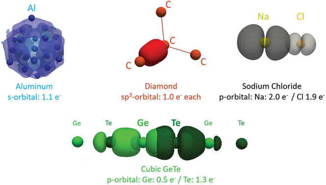
Revisiting the Nature of Chemical Bonding in Chalcogenides to Explain and Design their Properties
Advanced Materials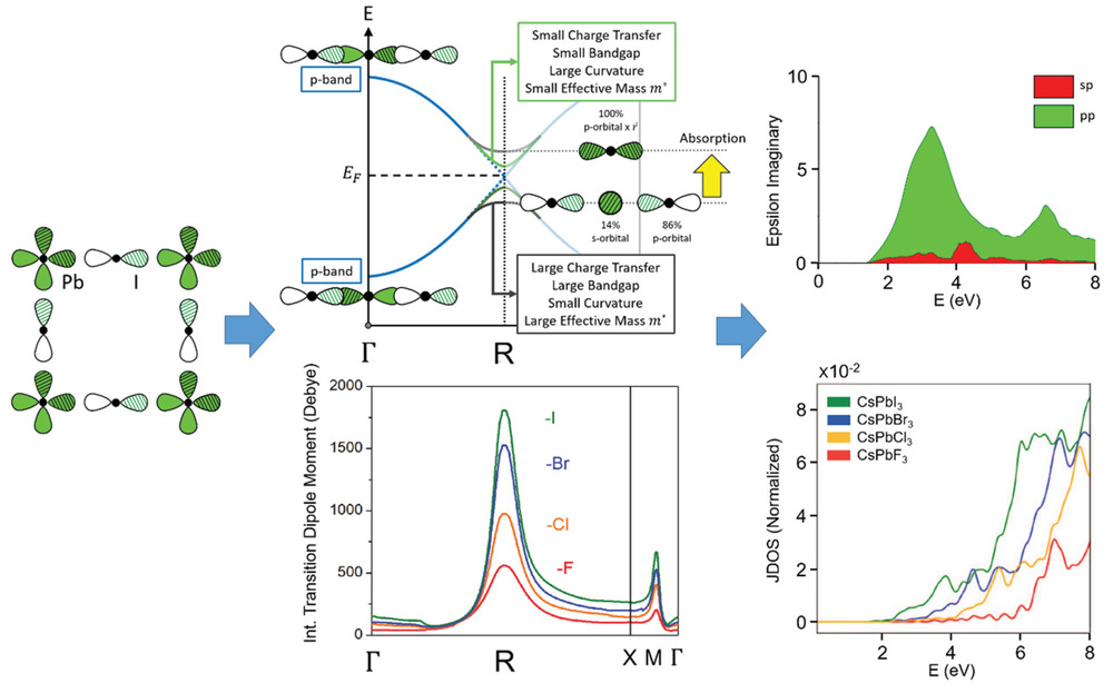
Halide Perovskites: Advanced Photovoltaic Materials Empowered by a Unique Bonding Mechanism
Advanced Functional Materials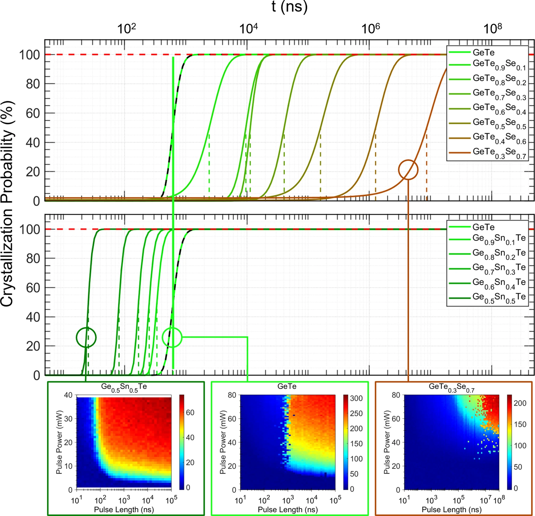
The potential of chemical bonding to design crystallization and vitrification kinetics
nature communications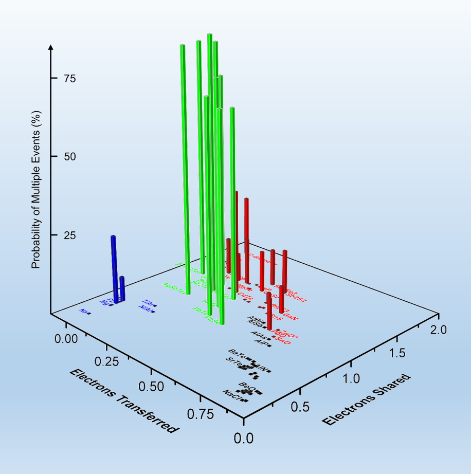
Chalcogenides by Design: Functionality through Metavalent Bonding and Confinement
Advanced Materials
Metavalent bonding in crystalline solids: how does it collapse?
arXiv
Chalcogenide Thermoelectrics Empowered by an Unconventional Bonding Mechanism
Advanced Functional Materials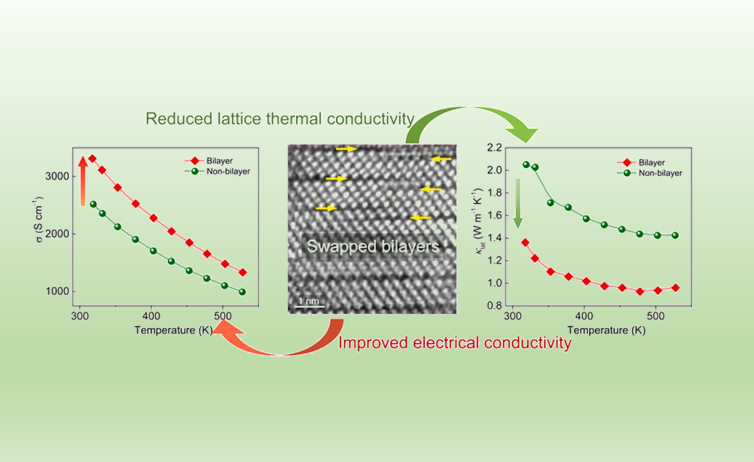
Enhancing thermoelectric performance of Sb2Te3 through swapped bilayer defects
Nano Energy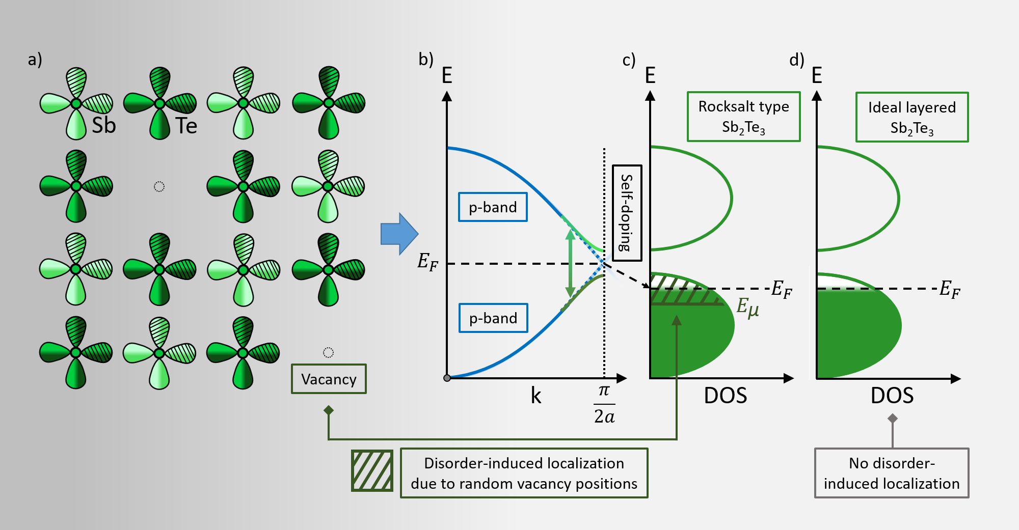
Materials Screening for Disorder-Controlled Chalcogenide Crystals for Phase-Change Memory Applications
Advanced Materials